
Lab
Our laboratory is equipped with specialized instrumentation for the characterization and integration of nanocarbon-based devices and sensors.
We also have access to cleanroom facilities (LMF, Polytechnique Montréal) equipped with state-of-the-art instrumentation for wafer-scale microfabrication, as well as different facilities for high-resolution microscopy and spectroscopy (SEM, AFM, Raman and XPS) for graphene and carbon nanotube characterization (LCM, UdeM and LASEM, Polytechnique Montréal).
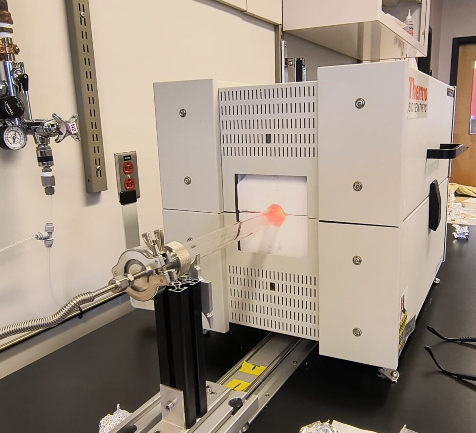
Chemical Vapor Deposition (CVD) furnace
Custom system enabling the growth of carbon nanotubes from catalyst particles on silicon substrates, in a ultra pure noble gas atmosphere and under ambient pressure. This system can also be used to perform vacuum annealing of chips.
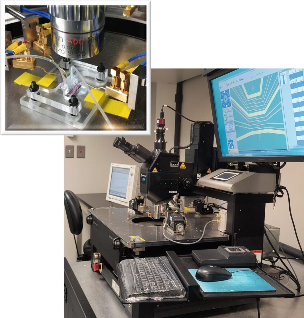
Probe station and semiconductor sevice parameter analyzer
The Keysight B1500A semiconductor parameter analyzer coupled to the Cascade Summit 12000 AP Probe Station, powered by Velox software, is a high-precision system designed for semi-automated operation, enabling high-throughput electrical characterization of chips and wafers.
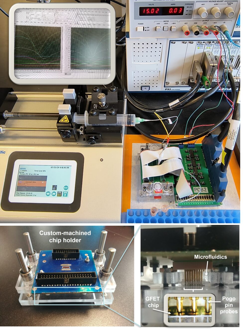
Multiplexed electrical measurement setup
custom instrumentation integrating multiplexed electrical probing and precise flow control. It features custom software for data acquisition and analysis, enabling parallelized addressing of up to 16 devices per chip. ( Bazan, 2022)
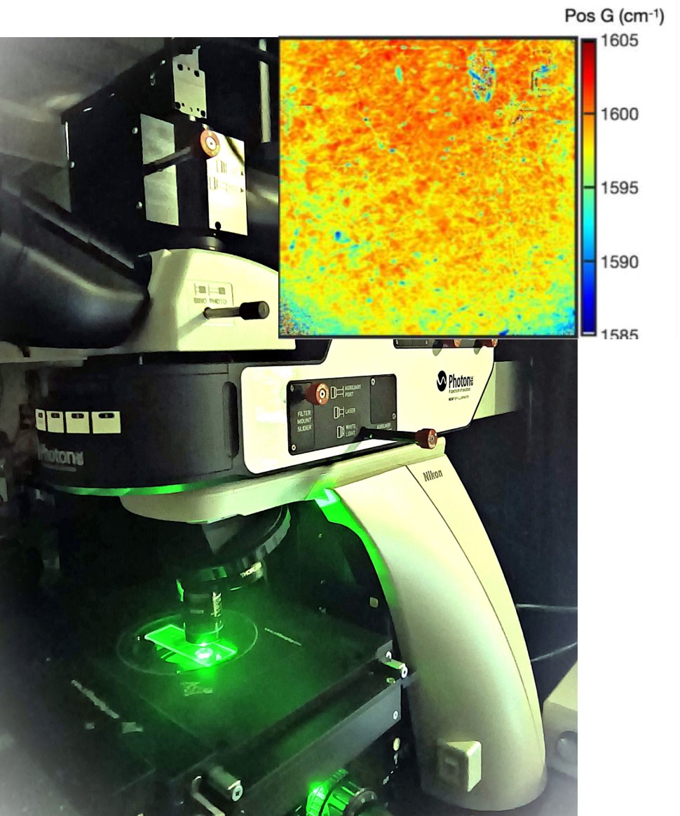
IMA VIS/IR hyperspectral Imager
The IMA is a hyperspectral microscope (Photon etc.) that combines spectral and spatial information, enabling rapid photoluminescence (PL) mapping for the optical and spatial characterization of a wide range of materials.
Automated graphene transfer setup
Custom automated system for the precise transfer of arrays of oriented graphene ribbons, enhancing reproducibility and scalability in device fabrication (Bencherif, 2024).
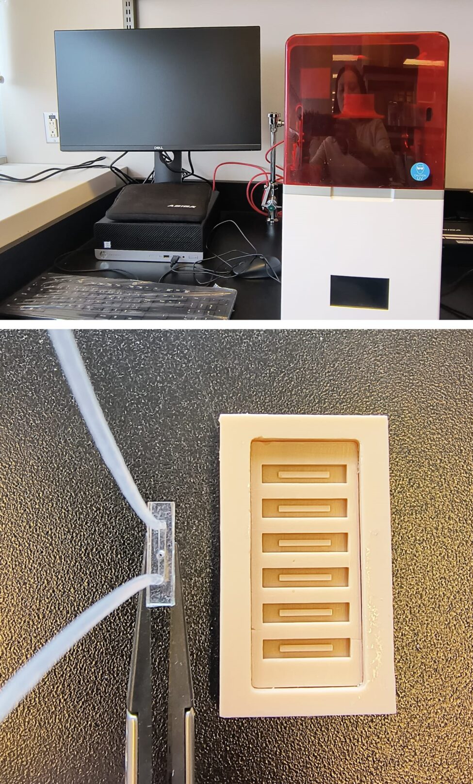
3D Printer & microfluidics
High resolution 3D printer enables stereolithography for the rapid prototyping of microfluidic molds for the integration of fluidic control.
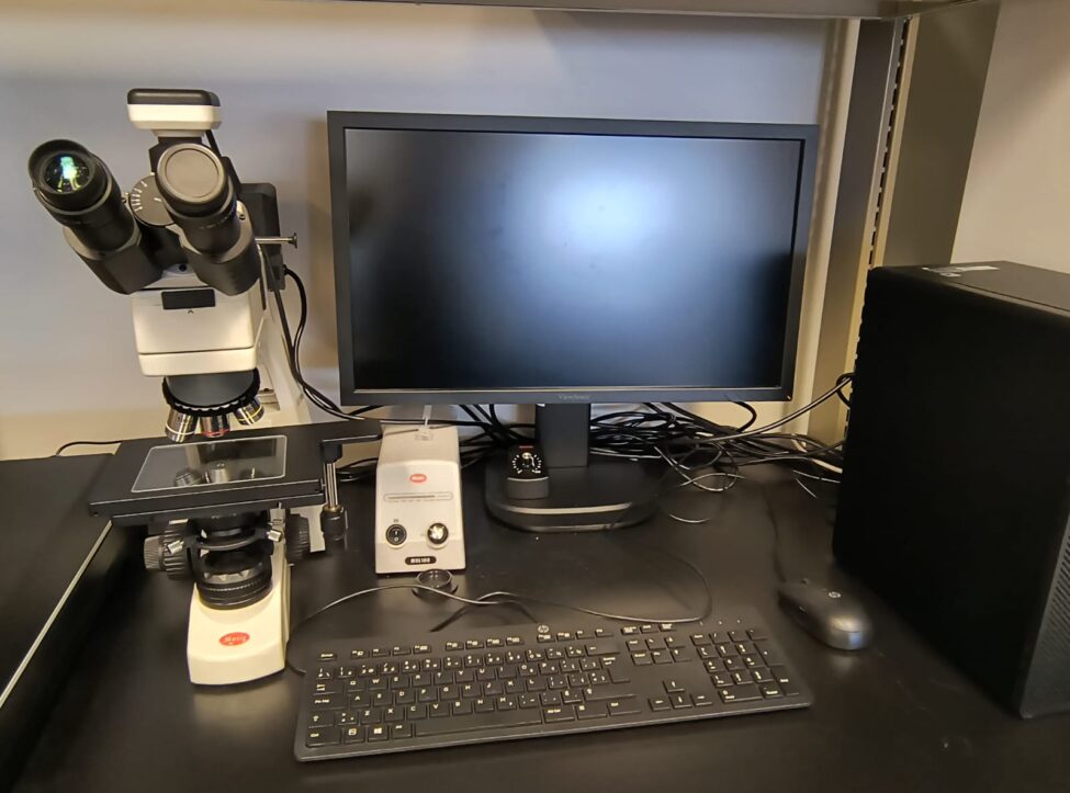
Optical microscope
Upright microscope in reflectance for the optical characterization (up to 100X) of graphene surfaces after chip fabrication, ensuring quality assessment and defect identification.
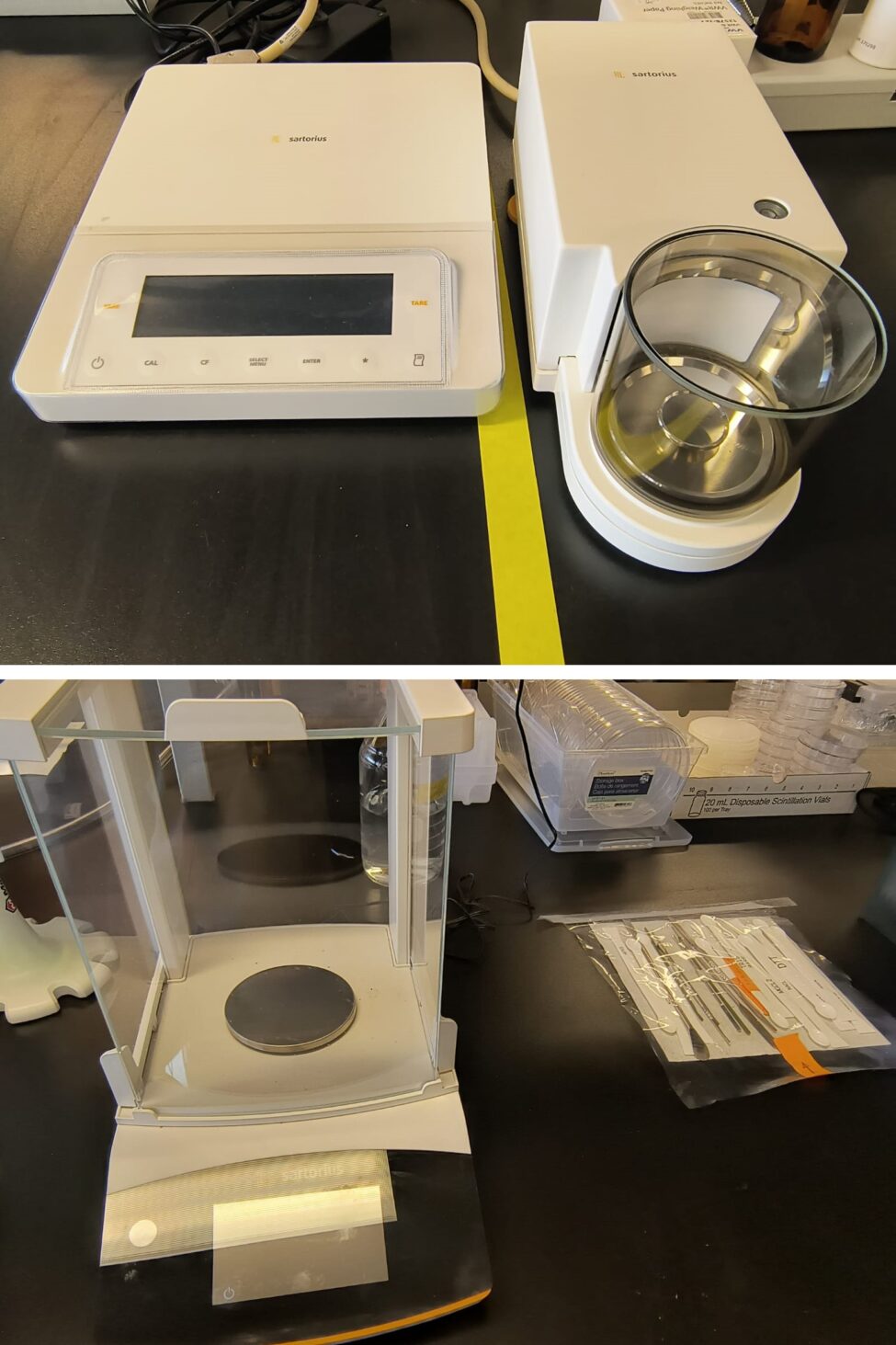
Weighing & Solution preparation workstation
High-precision 5-digit resolution analytical balance.
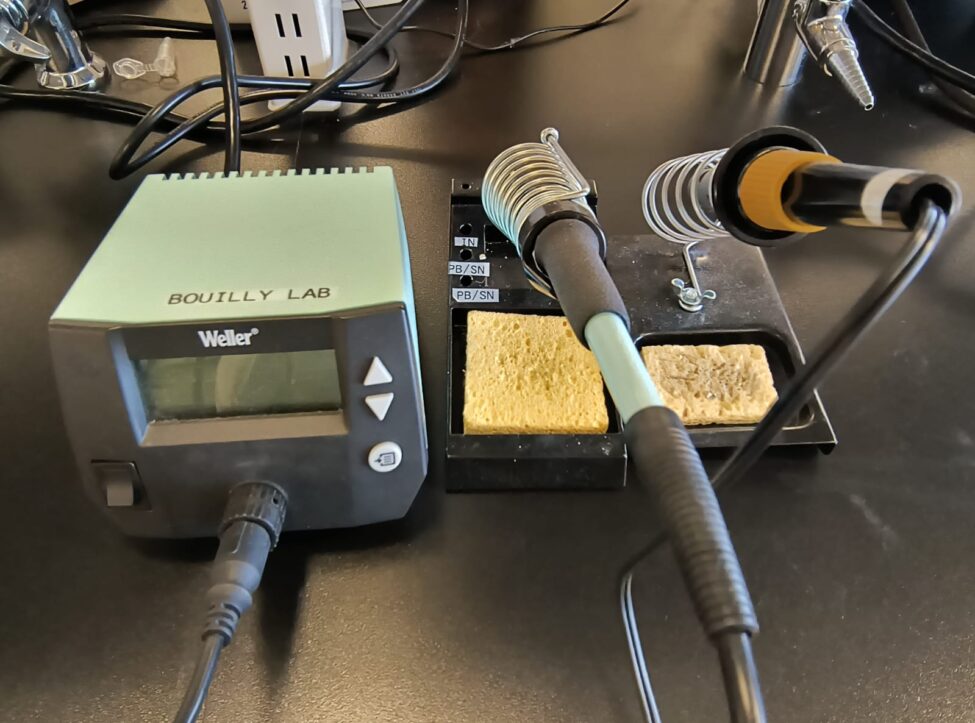
Soldering workstation
General soldering work of lab-made printied circuit boards (PCBs).
Ce contenu a été mis à jour le 2 septembre 2025 à 20h17.
This content has been updated on 16 March 2026 at 16h14.